T: +86-518-85528012
E: nick@luverrequartz.com
E: nick@luverrequartz.com
1st floor Runlian industrial center No. 116 QuFeng Rd., Haizhou Economic and technological development zone Lianyungang City, Jiangsu Province, China 222062
High transmittance semiconductor packaging quartz glass plate
High transmittance semiconductor packaging quartz glass plate, also known as semiconductor glass wafer, is an inorganic non-metallic material used for semiconductor packaging.
LUVERRE quartz
99.99%
Inner with Vacuum PVC bag and then wrapped with air bubble film, outer with wooden box.
as per customer's requirement
| Availability: | |
|---|---|
High transmittance semiconductor packaging quartz glass plate
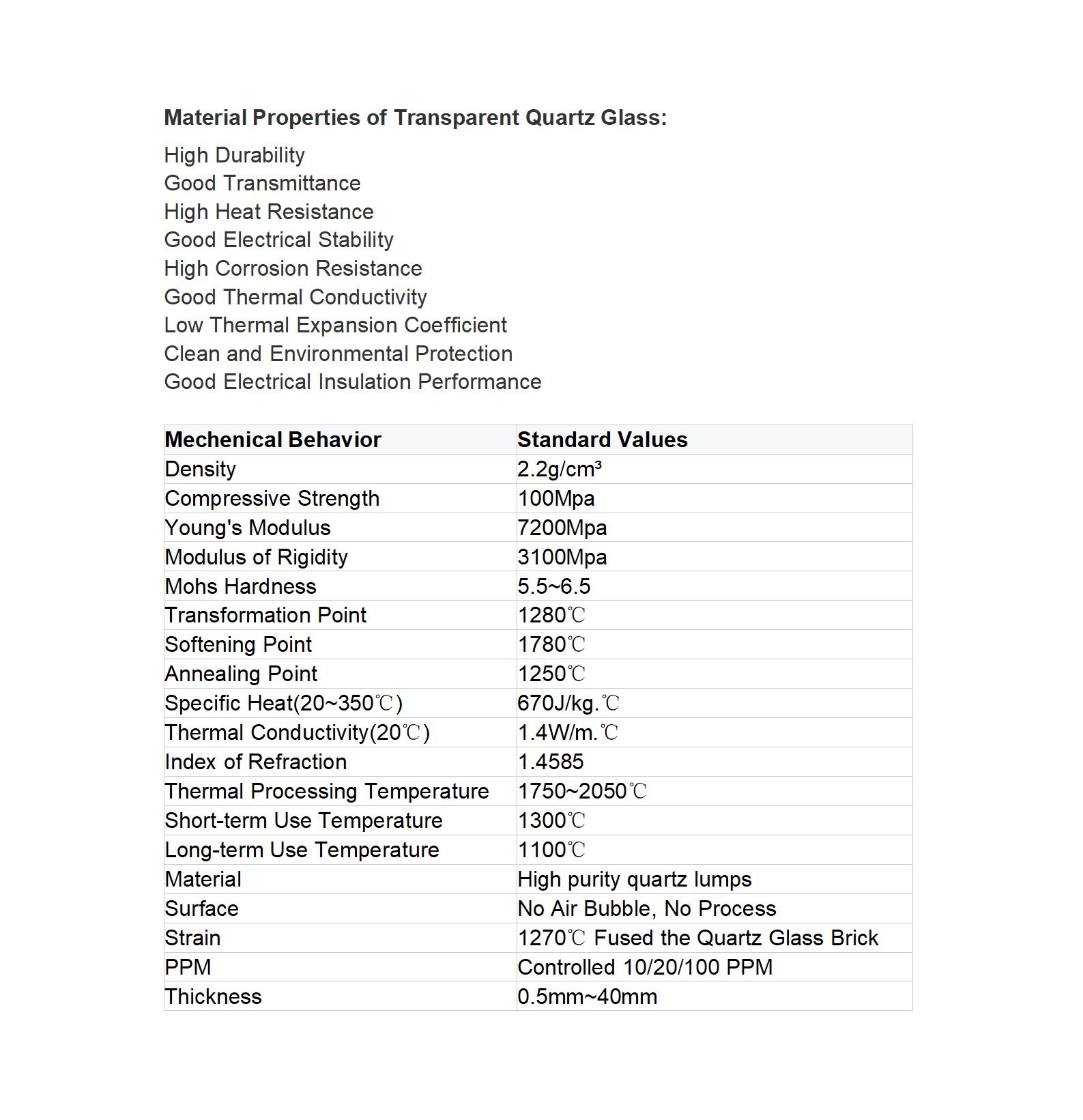
High transmittance semiconductor packaging quartz glass plate, also known as semiconductor glass wafer, is an inorganic non-metallic material used for semiconductor packaging. This material has attracted industry attention and recognition due to its unique properties.
High transparency: The high transparency of glass substrates makes them suitable as optical windows for packaging optical sensors. This makes it an important component in semiconductor packaging.
High thermal stability and chemical stability: Glass substrates can maintain stable performance in harsh environments such as high temperature and high humidity, ensuring the reliability of semiconductor devices.
Excellent electrical insulation performance: This helps prevent electrical faults and improve the safety of semiconductor devices.
Good processing performance: Glass substrates can be precisely cut, punched, and ground as needed to meet various packaging requirements.
![]()
Applications in semiconductor packaging include:
Chip packaging: As a substrate material for chips, it provides good electrical insulation and mechanical support.
Sensor packaging: Especially for optical and chemical sensors, the high transparency and chemical stability of glass substrates make them an ideal choice.
LED packaging: The high thermal stability and transparency of glass substrates help improve the luminous efficiency and heat dissipation performance of LEDs.

Although glass substrates have many advantages in the field of semiconductor packaging, they also face some challenges, such as cost issues and processing difficulties.